Open-Source IC Design & Precision Sensing

From open silicon to
deployed systems

Silicon2Systems

We design custom analog and RF integrated circuits on open-source PDKs — and carry that silicon through to complete FMCW radar, GNSS receiver, and AIS tracking systems engineered for industrial deployment.

SkyWater 130nmSKY130 Open PDK
GlobalFoundries 180nmGF180MCU Open PDK
IHP 130nm SiGeSG13G2 BiCMOS
Architecture
A complete value stack
silicon to systems

A single integrated path from open foundation PDKs through custom silicon to deployed precision sensing — with proprietary barriers eliminated at every layer.

Silicon to Systems architecture diagram Three-tier blueprint showing open-source PDKs and EDA tools at the foundation, custom silicon in the middle, and deployed FMCW radar, GNSS, and AIS systems at the top — with barriers like NDAs, license fees, and proprietary IP eliminated between layers. TIER 03 DEPLOY TIER 02 DESIGN TIER 01 FOUNDATION // DEPLOYED PRECISION SYSTEMS FMCW Radar Sub-meter range · all-weather SENSING GNSS Receiver NavIC L5 + S-band POSITIONING AIS Tracking Maritime · IMO compliant IDENTIFICATION // CUSTOM SILICON DESIGN Custom Analog & RFIC Schematic · Layout · DRC/LVS · GDSII · Tapeout RF / ANALOG DIGITAL MIXED-SIGNAL DSP / / BARRIERS REMOVED / / No NDAs Zero License Fees Proprietary IP Lock-in // OPEN-SOURCE FOUNDATION SKY130 130nm SkyWater Open PDK CMOS · OPEN GF180MCU 180nm GlobalFoundries Open PDK CMOS · OPEN IHP SG13G2 130nm IHP SiGe BiCMOS Open PDK SiGe · OPEN A B C
A

Deploy Layer

Field-ready FMCW radar, GNSS receivers, and AIS tracking modules engineered for industrial environments.

B

Design Layer

Custom analog and RFIC silicon designed end-to-end on a zero-license open EDA toolchain.

C

Foundation Layer

Open-source process design kits — Sky130, GF180MCU, and IHP SG13G2 — accessible without proprietary friction.

Open-Source IC Design
Zero-license ASIC design,
schematic to GDSII

Complete IC development on open-access PDKs. We eliminate proprietary EDA lock-in and deliver fabrication-ready designs at a fraction of traditional cost.

Custom RFIC layout — dual transformer-coupled architecture with octagonal inductors and pad ring
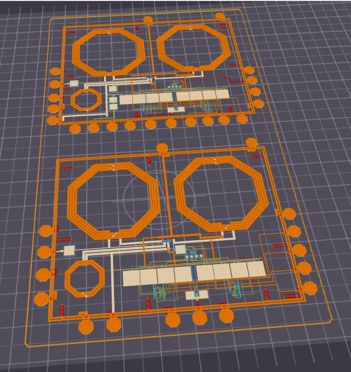
Inductors / RF passives
Active devices
Pad ring
01

Custom ASIC & RFIC

Full-cycle IC development — schematics, layout, DRC/LVS verification, GDSII generation, tapeout coordination, and post-fab silicon bring-up.

02

Zero-License EDA Flow

Entire design flow on open-source tools — no NDAs, no royalties, no vendor lock-in. Up to 90% reduction in EDA licensing costs.

03

MPW & Prototyping

Affordable silicon access through multi-project wafer shuttles and tile-based prototyping on supported foundry nodes.

04

Workforce Training

Fabrication-oriented VLSI programs — participants work with real PDKs and produce actual fabricated chips. Digital-first labs, no proprietary software.

90%
EDA Cost Reduction
3 PDKs
Supported Foundry Nodes
0 Licenses
Required to Start
Why Open-Source Silicon
Critical infrastructure deserves
access without barriers

The high-entry-barrier sectors that need precision sensing most — autonomous platforms, transport safety, maritime security, semiconductor research — are systematically locked out by traditional IC design economics. Open silicon changes the equation.

Cost Barrier

Bypassing legacy EDA toolchain economics

Proprietary EDA suites carry six-figure annual licenses per seat — pricing out startups, research labs, and entire emerging ecosystems. Our zero-license open EDA flow runs the complete design cycle on freely auditable tools, redirecting that capital into actual silicon.

Up to 90% reduction in design tool spend
Speed Barrier

No NDAs. No legal friction. No waiting.

Conventional foundry PDKs are gated behind multi-month NDA negotiations and export controls. Sky130, GF180MCU, and IHP SG13G2 are accessible from day one — letting design and validation begin while traditional projects are still in legal review.

Months of negotiation eliminated
Access Barrier

Affordable silicon enables critical systems

When R&D cost falls, who can build changes. Lower silicon cost makes precision FMCW radar, GNSS, and AIS modules economically viable for industrial applications, smaller agencies, and academic research — not only for tier-1 corporate budgets.

Critical infrastructure within reach
Value Hierarchy
Three layers, one unified mission

From open-source foundations to deployed precision systems — every layer of the Silicon2Systems stack reinforces independence, affordability, and access for industrial and commercial operators.

Silicon2Systems value pyramid A three-tier pyramid showing the Silicon2Systems value hierarchy: open-source foundation at the base, custom silicon IP in the middle, and deployed precision sensing systems at the top. Critical Sensing Systems Custom Silicon IP Analog & RFIC ASICs (CHIPS) Open-Source EDA & Open PDKs SKY130 · GF180 · IHP SG13G2 (FOUNDATION) 03 02 01
03

System Integration

Building precision sensing systems on indigenous silicon — FMCW radar, GNSS receivers, and AIS modules engineered for industrial deployment, fully traceable from die to deployed unit.
02

Silicon Independence

Building libraries of custom analog and RFIC IP — owned, auditable, and reusable. Each block becomes part of a growing portfolio of independent silicon assets.
01

Zero-License Foundation

Designing ASICs on Sky130, GF180MCU, and IHP SG13G2 open ecosystems — eliminating commercial EDA costs entirely while training the next generation of silicon engineers.
High-Precision Sensing
Three sensing domains,
one integrated stack

From electromagnetic sensing to satellite positioning and maritime identification — each system engineered for sub-system integration.

Electromagnetic Sensing

FMCW Radar

Frequency-Modulated Continuous Wave radar delivering sub-meter range resolution for object detection, terrain mapping, and perimeter monitoring across all weather conditions.

Resolution< 1m range
ProcessingSoftware-defined
ConditionsAll-weather
Satellite Positioning

GNSS Receivers

Dual-band RF front-end architecture for NavIC (L5 & S-band). Custom RFIC on Tower 180nm CMOS/RFCMOS with integrated low-noise amplifier stages for precision positioning.

BandsL5 + S-band
ConstellationNavIC / GPS
ProcessTower 180nm
Maritime Identification

AIS Tracking

Automatic Identification Systems for real-time vessel tracking, port security, and coastal surveillance — designed for integration with existing vessel traffic service infrastructure.

StandardIMO compliant
IntegrationVTS compatible
CoverageCoastal + port
Application Sectors
Where our silicon
becomes systems
Industrial

Autonomous Systems

FMCW radar and GNSS modules for autonomous navigation, obstacle avoidance, and precision positioning in industrial environments.

Maritime

Port & Coastal Security

AIS vessel tracking and radar-based surveillance for port authorities, coast guard operations, and maritime traffic management.

Transport

Railway Safety

Anti-collision avoidance systems for high-speed rail networks — FMCW sensing with real-time obstacle detection and alerting.

Semiconductor

Open-Source IC Ecosystem

Custom ASIC services, MPW shuttles, and fabrication-oriented workforce training for startups, research labs, and academia.

Leadership
Built by engineers,
40+ years combined
V

Vipul

CEO & Co-Founder

21 years in Analog & RFIC VLSI design. Scientist & Engineer at SCL, establishing RFIC design flows and silicon measurement setups. End-to-end IC development from schematics to GDSII to post-fab validation. Designed NavIC dual-band RF front-end on Tower 180nm CMOS/RFCMOS and multiple IPs across open-source PDK ecosystems.

N

Nakul

Co-Founder & CTO

21+ years in RF MEMS, antenna design, and manufacturing. Developed RF MEMS-based micro antennas and phased array systems for satellite and 5G communications. 24+ patents granted in the RF domain.